
SEMICONDUCTOR EQUIPMENT
Precision Ceramics
for the Semiconductor Industry
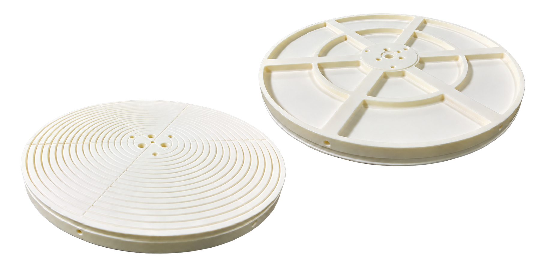
Precision ceramic components for wafer processing and handling, process chambers, and equipment structures. Our range includes carriers, vacuum chucks, grinding plates and dressing rings, handling arms, etching chamber components, and structural parts.
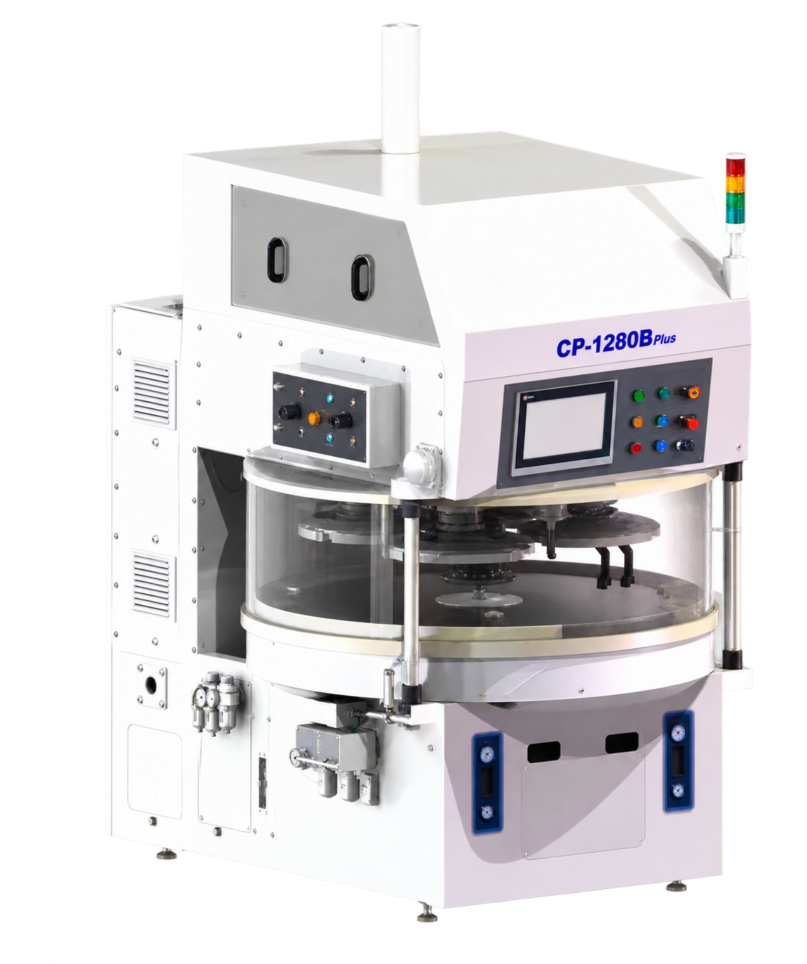
99.5% Alumina Ceramic Carrier
Product Features
Made from high-purity, ultrafine alumina powder and sintered at high temperatures, this ceramic carrier offers high purity, low impurity levels, high hardness, wear and corrosion resistance, and electrical insulation. The material has a low coefficient of thermal expansion and a high elastic modulus. Precision machining and dimensional stability make the carrier suitable for ultraprecision processing of semiconductor wafers.
Applications
Primarily used for thinning, hard polishing, and chemical mechanical polishing (CMP) of LED substrates and semiconductor wafers, including sapphire, silicon carbide, silicon, germanium, gallium arsenide, and gallium nitride wafers.
Technical Specifications
| Parameter | Value |
|---|---|
| Maximum outer diameter (mm) | Ø635 mm |
| Parallelism (mm) | 0.001–0.005 mm |
| Flatness (mm) | 0.001–0.005 mm |
| Surface roughness, Ra (μm) | 0.1–0.2 μm |
| Al₂O₃ content (%) | ≥99.5% |
| Density (g/cm³) | ≥3.92 g/cm³ |
| Wear volume loss (cm³) | ≤0.4 cm³ |
| Hardness (HRA) | ≥90 HRA |
| Flexural strength (MPa) | >400 MPa |
Long Ceramic Plate
Product Features
Made from high-purity, ultrafine alumina powder and sintered at high temperatures, this long ceramic plate offers high purity, low impurity levels, high hardness, chemical stability, wear and corrosion resistance, and electrical insulation. Precision machining produces accurate dimensions that remain stable during use.
Applications
Used as base components in coating equipment for large glass substrates in liquid crystal display (LCD) manufacturing, and as support brackets in semiconductor material-handling equipment. These applications require excellent corrosion resistance, thermal stability, and strength.
Technical Specifications
| Parameter | Value |
|---|---|
| Maximum length (mm) | 2,100 mm |
| Al₂O₃ content (%) | ≥99.0% |
| Density (g/cm³) | ≥3.90 g/cm³ |
| Wear volume loss (cm³) | ≤0.4 cm³ |
| Hardness (HRA) | ≥90 HRA |
| Flexural strength (MPa) | >400 MPa |
| Acid resistance (%) | 99.8% |
| Alkali resistance (%) | 99.8% |
Related Structural Components
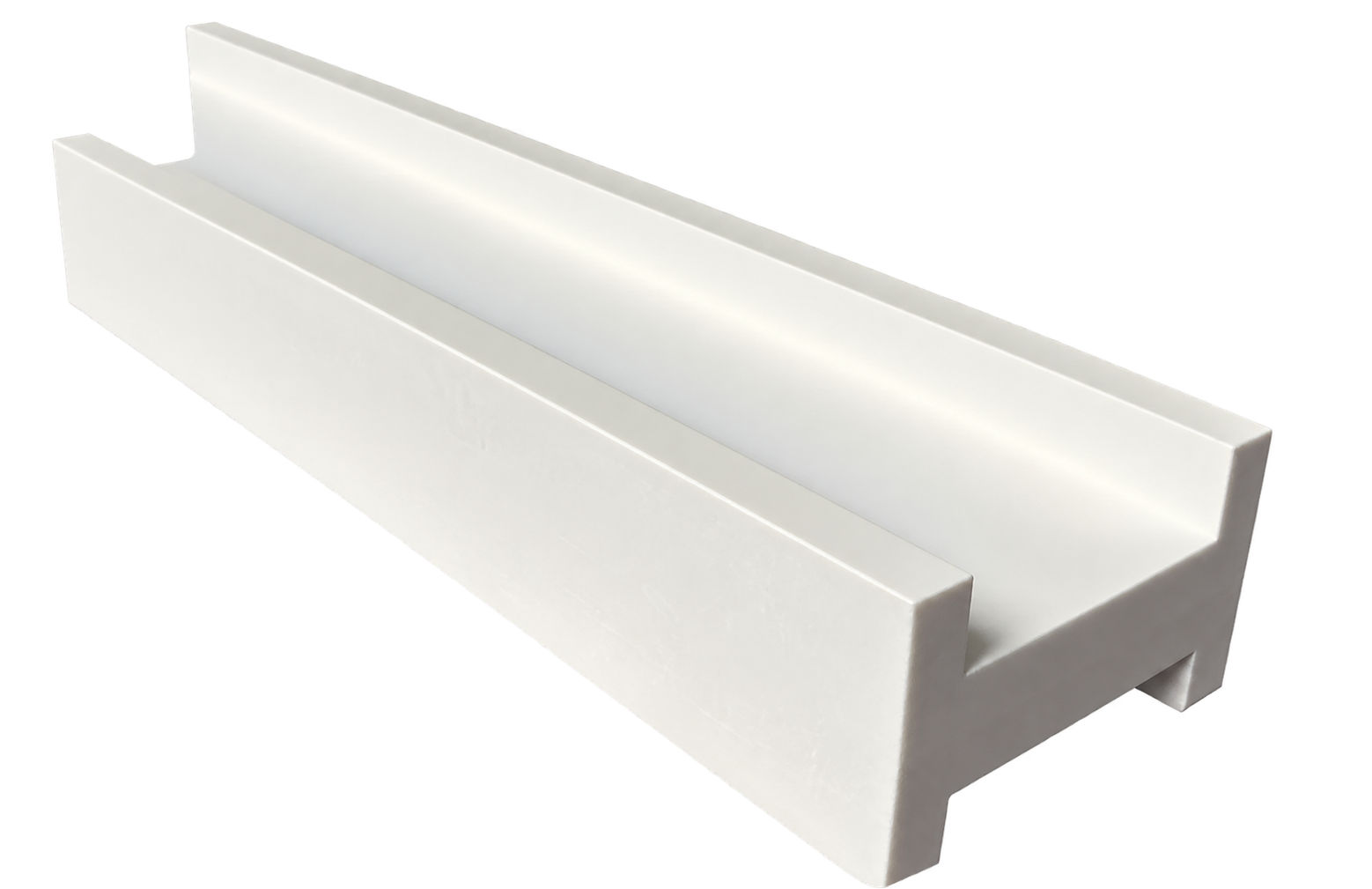
Ceramic Bracket
- Available Sizes
- 2,000 × 165 × 30 mm
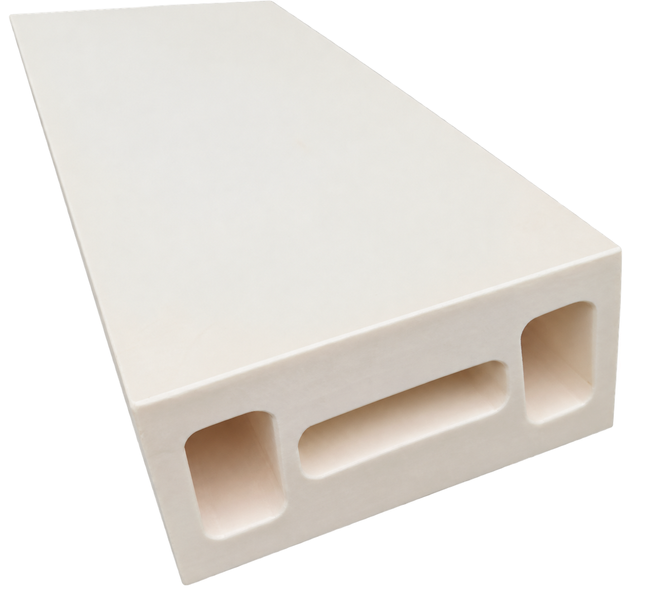
Ceramic Guide Rail
- Dimensions
- 200 × 90 × 1,160 mm
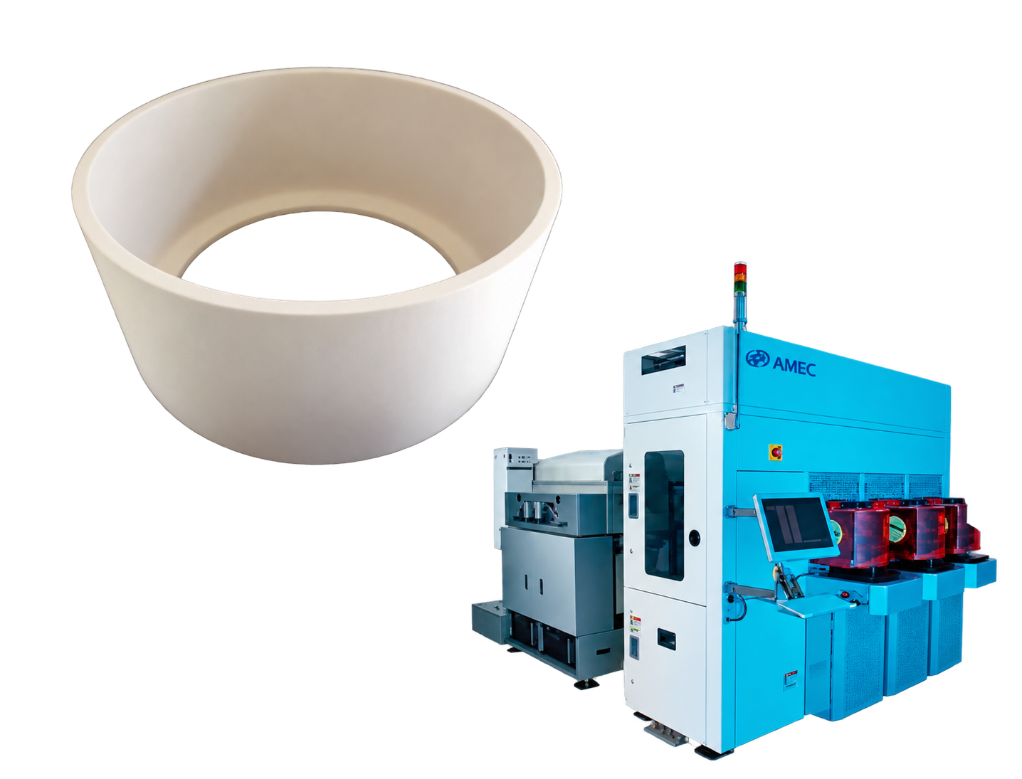
Plasma Etching Chamber Components
Product Features
Manufactured from high-purity, ultrafine alumina powder by isostatic pressing and high-temperature sintering, these components feature high material purity, fine grains, a dense and uniform microstructure, chemical stability, and corrosion resistance. Uniform density, consistent impedance characteristics, and low dielectric loss support stable plasma etching performance.
Applications
Used in etching and plasma-enhanced chemical vapor deposition (PECVD) equipment for wafer manufacturing.
Technical Specifications
| Parameter | Value |
|---|---|
| Maximum outer diameter (mm) | Ø650 mm |
| Al₂O₃ content (%) | ≥99.0% |
| Density (g/cm³) | ≥3.90 g/cm³ |
| Hardness (HRA) | ≥90 HRA |
| Flexural strength (MPa) | >400 MPa |
| Acid resistance (%) | 99.8% |
| Alkali resistance (%) | 99.8% |
Ceramic Handling Arm
Product Features
Made from high-purity, ultrafine alumina powder and sintered at high temperatures, these ceramic components offer high hardness and resistance to wear and corrosion. The precision-machined parts offer high rigidity, low thermal deformation at elevated temperatures, and a long service life.
Applications
Widely used in LED, semiconductor, and photovoltaic applications, as well as packaging, testing, and wafer processing.
Technical Specifications
| Parameter | Value |
|---|---|
| Al₂O₃ content (%) | ≥99.0% |
| Density (g/cm³) | ≥3.90 g/cm³ |
| Wear volume loss (cm³) | ≤0.4 cm³ |
| Hardness (HRA) | ≥90 HRA |
| Acid resistance (%) | 99.8% |
| Alkali resistance (%) | 99.8% |
Other Precision Ceramic Components
Product Features
Made from high-purity, ultrafine alumina powder and sintered at high temperatures, these ceramic components offer high purity, high hardness, and resistance to wear and corrosion. The precision-machined parts offer low contamination potential, high rigidity, low thermal deformation at elevated temperatures, and a long service life.
Applications
Widely used in LED, semiconductor, and photovoltaic applications, as well as packaging, testing, and wafer processing.
Technical Specifications
| Parameter | Value |
|---|---|
| Maximum outer diameter (mm) | Ø650 mm |
| Al₂O₃ content (%) | ≥99.0% |
| Density (g/cm³) | ≥3.90 g/cm³ |
| Wear volume loss (cm³) | ≤0.4 cm³ |
| Hardness (HRA) | ≥90 HRA |
| Acid resistance (%) | 99.8% |
| Alkali resistance (%) | 99.8% |
ADDITIONAL SEMICONDUCTOR COMPONENTS
Vacuum Holding & Wafer Processing
Porous Ceramic Vacuum Chucks
Used in the manufacture of silicon, sapphire, gallium arsenide, and other semiconductor wafers.
- Available Sizes
- Ø8 in.; Ø12 in.
Vacuum Chuck for Wafer Chamfering
For use in chamfering machines for the semiconductor industry.
- Available Sizes
- Ø280 × 20 mm
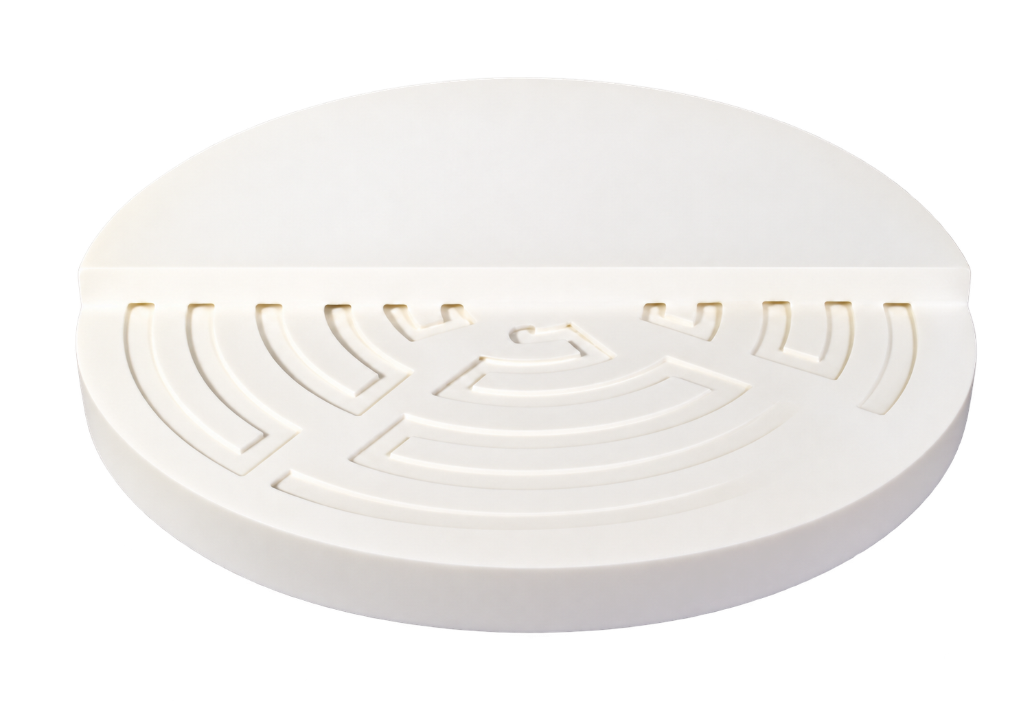
Hollow Ceramic Plate
For semiconductor applications.
- Available Sizes
- Ø365 × 40 mm
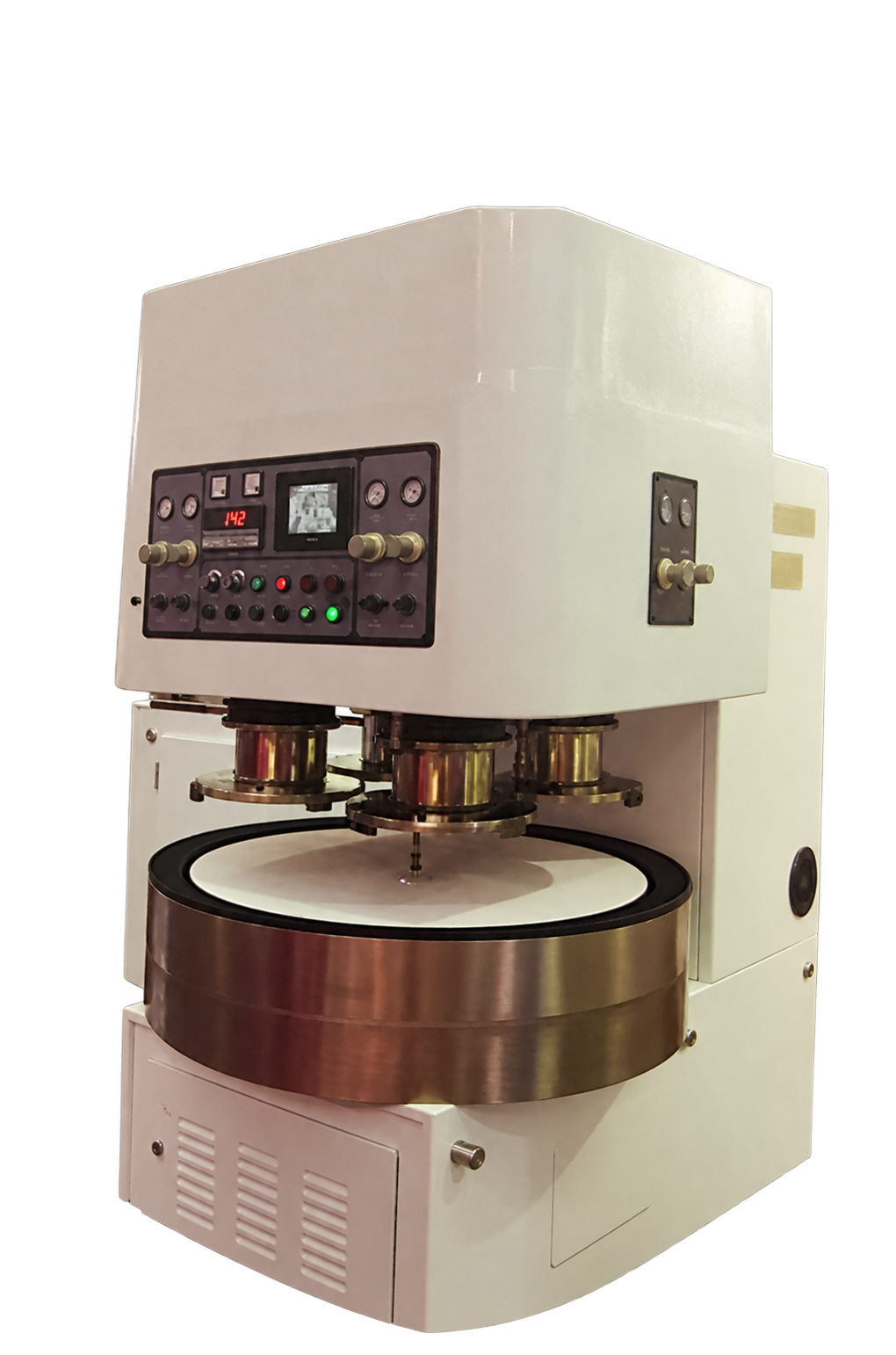
Ceramic Grinding Plates & Dressing Rings
For semiconductor applications.
- Available Sizes
- Ø800 mm, Ø610 mm, Ø590 mm, Ø520 mm, Ø485 mm, and Ø360 mm
MATERIALS FOR THE SEMICONDUCTOR INDUSTRY
Why use alumina ceramics in the semiconductor industry?
Precision, particle control, and electrical isolation are central to semiconductor equipment design. Alumina ceramics can help meet these needs when the grade, surface finish, and component geometry are matched to the process.
Limit particles from wafer contact
Smooth, wear-resistant ceramic contact surfaces help reduce particle generation during wafer handling. Surface finish and cleanliness are critical to protecting the wafer.
Match the chamber chemistry
High-purity alumina is used in semiconductor process chambers. Resistance to chemical and plasma attack depends on the ceramic grade and process conditions, so compatibility must be evaluated for the intended environment.
Maintain accurate wafer positioning
Stiff ceramic arms and supports help maintain positioning accuracy during wafer transfer. Dimensional tolerances and thermal expansion must be considered together in the equipment design.
Combine insulation with structural support
Alumina provides electrical insulation as well as mechanical support. Its dielectric properties make it useful for insulating components in semiconductor equipment.